Understanding Wave Soldering
Wave soldering is a high-volume electronic manufacturing process used to create reliable solder joints between electronic components and printed circuit boards (PCBs). This automated process is commonly employed in the assembly of PCBs, especially in the production of consumer electronics, automotive components, and communication devices.

How Does Wave Soldering Work?
Wave soldering involves several key steps:
- Preparation: The PCB is first coated with a layer of flux to help facilitate the soldering process by preventing oxidation and improving wetting of the solder.
- Component Placement: Components are placed onto the PCB either manually or through automated pick-and-place machines.
- Conveyor System: The PCB is loaded onto a conveyor belt and passed through a series of stations that include fluxing, preheating, solder wave, and cooling.
- Fluxing: The fluxing station applies flux to the PCB, ensuring that the surfaces of the components and PCB are properly coated.
- Preheating: The preheating zone heats the PCB to a specific temperature to prepare it for soldering, which helps reduce thermal shock to the components.
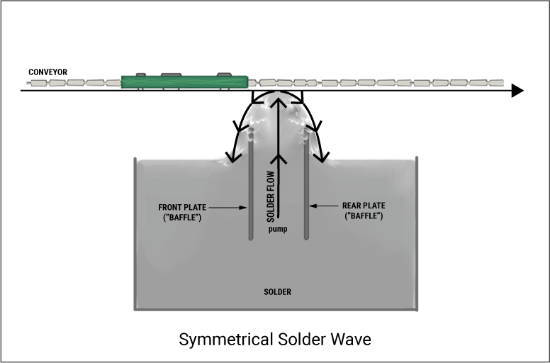
- Solder Wave: The heart of the wave soldering process, this stage involves passing the PCB over a wave of molten solder. The wave can be shaped like a ramp, and its height and speed can be adjusted according to the specific requirements of the assembly.
- Cooling: After the solder wave, the PCB passes through a cooling tunnel that solidifies the solder joints, securing the components to the PCB.
What are the Key Benefits of Wave Soldering?
- Efficiency: Wave soldering allows for high-speed and automated production, significantly increasing throughput and reducing labor costs.
- Consistency: This process ensures consistent solder joint quality and reliability, which is crucial for electronic assemblies.
- Cost-Effective: The ability to solder multiple joints simultaneously reduces per-unit costs, making wave soldering a cost-effective option for mass production.
- Versatility: Wave soldering can be adapted for various types of PCBs, including single and double-sided boards, making it a flexible solution for different manufacturing needs.
What are the Common Challenges in Wave Soldering?
- Thermal Damage: Excessive heat can damage sensitive components and cause issues like solder bridging or component lifting.
- Flux Residue: Residual flux can cause reliability issues and might require additional cleaning steps.
- Solder Joint Defects: Poor soldering practices can lead to defects such as poor wetting, cold joints, or insufficient solder.
Conclusion
Wave soldering is a powerful tool in the field of electronics manufacturing, offering high efficiency, consistency, and cost-effectiveness. Understanding the process, its benefits, and potential challenges is essential for anyone involved in the production and assembly of electronic components. With continuous advancements in technology, wave soldering remains a key process in the quest for more reliable and cost-effective electronic assemblies.